IOTA Crypto Core FPGA — 1st Progress Report
This is my first progress report about my EDF-funded project the IOTA Crypto Core FPGA. I try to do one every 4 weeks until all milestones are finished …^^


About the project
IOTA core functions like address generation, signing, “Mini-Pow” and Proof of Work (PoW) need much computational power which makes it almost impossible (in a practical sense) to be done by small embedded systems.
The aim of the project is to develop several modules that can be use by existing or new embedded applications needing IOTA core functionality.
The first is an IOTA Core FPGA module which provides most IOTA core functions with hardware acceleration. It will offer a high-level API which is easy to use whereas computationally intense low-level calculations are off-loaded to specialized logic which gives significant advantage in speed compared to a software-only solution — making it perfect for embedded applications.
Additionally, the FPGA module implements several security mechanisms which will make it very hard for attackers to unauthorizedly gain access of seeds which are stored on the module.
The second module will be a System-on-Module (SoM) which will use the FPGA module. This SoM will have enough resources to use it for a large number of applications. It even could run Linux. The SoM could be seen as an integration example for the FPGA module. It can be used unmodified for own applications but other microcontrollers could be using the FPGA module easily as well.
The third module is an application board using the SoM which will be an IOTA sensor gateway for simple and cheap sensors.
Overall, the architecture looks like this:

Currently, I’m working on the second milestone (the first was PiDiver PoW) which will be the actual FPGA core. A stock-FPGA board is used for this task and a SoC-system will be developed.
FPGA is an abbreviation for “Field programmable gate array”. It consists of Logic-blocks which can be configured inside the FPGA to build larger logic-functions up to complete CPUs. Such logic is described in a programminglanguage like Verilog or VHDL which then is synthesized to logic by synthesis tools. The most known FPGA manufacturers Xilinx and Altera offer complete IDEs for free (for small to mid-range FPGAs). FPGAs have some advantages because you can describe true parallel working logic — but you also can describe serially executed logic by using state-machines. But FPGAs are not good for everything because often it is better to use a microcontroller for certain tasks because logic-utilization can easily explode when trying to do everything in Verilog or VHDL. For such cases there are soft-cpus (e.g. from ARM) which can be used inside the FPGA.
This project uses such a soft-cpu (Cortex M1) which is combined with hardware-accelerators. These accelerators are logic-blocks (described in VHDL) which can do one task very fast — but nothing else (like SHA3). They can be integrated into the 32Bit address-space of the CPU which gives a very good coupling and quick transfer times.
The system looks like this in the BlockDesigner of Xilinx Vivado:
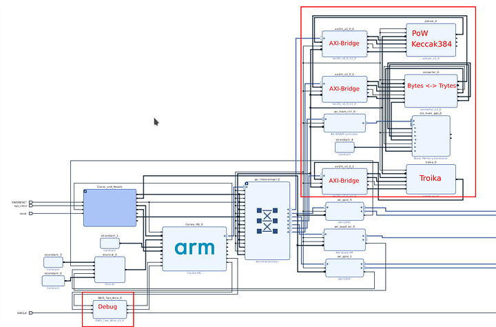
(the red components have been developed — the other were available as IPs in the catalog or were part of the example design)
Comparisons
In the following sections comparisons between Cortex M1 without accelerators, Cortex M1 with accelerators, Cortex M3, Cortex M4, Raspberry Pi 3B and my desktop PC (an Core i5) are shown.